Fundamental And Types Of Capacitors

4:41 PM, Posted by electronikcircuit, No Comment

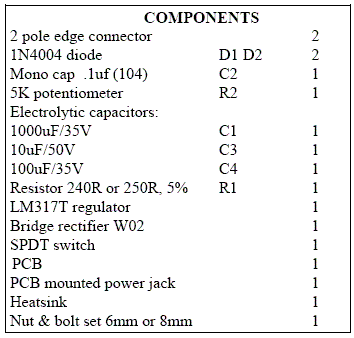
Introduction To Capacitors

A capacitor is a body which can store an electrical charge. It consists of 2 conducting plates facing each other and separated by an insulating material. This insulating material is also called dielectric material. When a charge is stored in one plate, an equal and opposite charge is inducted on the other plate and thus a potential difference is set up between the plates.

The unit of measurement for capacitance is Farad but this unit is much too large for practical work. It is usually measured in microfarads(uF) or picofarads(pF). The formula of calculating capacitance is

C= [(0.224 KA)(n-1)]/d where


C = capacitance in pF
K = dielectric constant of material between plates
A = area of one side of the plates square inches
d = separation of plate in inches
n = number of plates

The potential difference V developed when a charge Q is stored depends directly on the value of Q and inversely with the capacitance C of the cap.

V = Q/C

They are used in timing circuits as it takes time for a cap. to be charged up. They are used to smooth varying DC power supplies by acting as a reservoir of charge. They are also used in filter circuits because they easily pass AC signals but they block DC signals.

DC Voltage Rating

The DC working voltage of a cap. is the maximum voltage which may be applied continuously on the electrodes of the cap. at the upper limits of the working temperature range. The peak value of an alternating voltage should not exceed this rating and have to be derated according the the FMEA as recommended in FMEA

Leakage Resistance

The dielectric of a practical cap. introduces power losses which can be represented by a small resistance connected in series with the cap. The insulating resistance is often greater than 3,000 Mohm.

Types Of Capacitors

There are many different types of cap. that are used for different types of applications. They are electrolytic cap., ceramic cap., tantalum cap., polyester cap., polystyrene cap. and safety cap.(namely X and Y types of cap.).

Electrolytic Type

Electrolytic cap. have leads that are marked with + or - signs. They have polarity and must be connected with the correct polarity. The values of the capacitance and voltage rating are are printed with on its body. The voltage rating can range from 5V up to 440V DC. Generally this type of capacitor is used as smoothing cap. in power supply regulation. The bigger the value of the cap. is, the less ripple the DC supply that has been rectified will be.

Ceramic Type

This type of capacitor is most commonly used and both through hole and surface mount types are available. Its application is mainly used in general digital circuit, as power supply bypass capacitor, converters (both for input and output), Smoothing capacitors, DC-DC converters, Switching power supplies (secondary side).

Figures below show the typical characteristics of this type of capacitor. It shows the construction and the temperature range and codes of the cap. The impedance vs frequency change is also shown.


Tantalum Type

Tantalum type have low voltage ratings and they are expensive but very small. Usually they are used in application where a large capacitance is needed in a small size.

Metallized Polyester Film Type

Metallized Polyester Film is used for general purpose applications. Some of the features are its Self-healing property and flame retardant epoxy resin coating. Its voltage ranges from 100V DC to 1250V DC.

Safety Type

This type is classified into classes like X and Y types. It is usually used on the live parts of the circuity. One of the applications is in the area of reducing the harmonics on inverter motor drives type of application. As safety is a main concern over here, usually this type of cap. has UL, VDE, SEMKO and other types of marking which certifies that it conform to the safety standard of a particular country.


Fundamentals of Batteries

4:36 PM, Posted by electronikcircuit, No Comment

Introduction

Batteries can be divided into two categories. The primary type is intended for one time use only and is disposed after the charge has dropped to a level that cannot be used. Primary type should not be discharged as heat will be generated within sealed cells. It will also damage the equipment as a consequent of fluid leakage. The storage or secondary type can be recharged many times and is reusable.

The rating of its capacity is ampere hours (Ah) which is a product of current drain and time.

If it become cold, it will have less charge available and some design to keep it warm before use. It may lose 70% of its capacity at cold extremes but will recover with warmth.

Primary Batteries

Carbon zinc is the most common primary cell in which the chemical oxidation converts the zinc into salts and electricity. When there is no current flowing, the oxidtion stops. If keep for a long period of time, the stored batteries will degrade and dry out where it will no longer able to supply the desired current. The time taken for the degradation without being used is called shelf life. It has a nominal voltage of 1.5V.

Alkaline types have longer capacity at low temperatures. Lithium type have nominal voltage of 3V/cell and has the best capacity, discharge, shelf life and temperature characteristics. Its setback is the high cost.

Silver Oxide and Mercury has voltages of 1.5 V and 1.4 V respectively and are used where constant voltage is desired at low currents over a long period of time. Their main used and applications are in hearing aids.

Storage Batteries

The most commonn type is nickel-cadmium(Ni-Cd) type with a nominal voltage of 1.2V/cell. If used carefully, it can be rechargable up to 500 times compared to alkaline type which is 50 times or so. The most widely used storage type is the lead-acid type in automobile.The lead acid battery is made up of plates, lead, and lead oxide with a 35% sulfuric acid and 65% water solution.

Gas escaping from it may be explosive and always keep flame away. It should not be subjected to unnecessary heat, vibration or physical shock. Frequent inspections for leak is recommended. The electrolyte is chemically active and conductive and may ruin electrical equipment if leaks occurred. Its acidity may be neutralized with sodium bicarbonate or baking soda.

In order to ensure that all the cells in NiCd reach a fully charged condition, it should be charged by a constant current of 0.1 C current level. It is around 50 mA for a AA size cells. Charging should be terminated after 15 hours at the slow rate. A built in circuit that will stop charging when 1.43V/cell is reached will enhance the life of the battery.

Electronic Ballast Design Project

4:33 PM, Posted by electronikcircuit, No Comment

Introduction To Electronic Ballast Design

Fluorescent Lamp was introduced commercially in the 1940s and was a success in small scale lighting replacing the use of tungsten incandescent bulb. It continued to be used in the 21st century and has since evolved into many variation of outlook, applications and control.

Two main functions of a fluorescent lamp ballast are providing a starting kick and to limit the current to its operating value for the tube that is being used. There are basically 2 types of ballasts namely magnetic ballast and electronic ballast design. The magnetic ballast uses a core and coil assembly transformer that provides a minumum functions of starting and operating the lamp. Hence it is not as efficient as the electronic ballast. Electronic ballast operates at high frequencies from 20kHz to 45kHz and uses electronics circuitry to optimize the operation of the lamp.

Instant start ballasts require an instant-start certified lamp and ignite a lamp in about 80 milliseconds or less using a high frequency electronic circuit. It starts the lamp without heating the cathodes by using a high voltage at around 600V. It is the most efficient energy type when used in installations where the lamps are not turned on and off regularly.

Rapid start ballasts precisely heat the cathodes and then ignite the lamp with a lower charge. In this way, it helps to prolong the life of the lamp but it uses more energy as the cathodes are heated up continuously during the operation of the lamp.

Programmed Start is an upgrade version of rapid start. It allows the cathodes to be preheated before applying the voltage to the lamps to strike an arc. This type gives the best life to the lamps and is used in applications where frequent ON/OFF of lights are required.

Electronic ballast must be designed, installed and operate in compliance with the CSA, UL and NEC requirements. As the installation and testing come in contact with hazardous voltage, only qualified personnel should perform the installation. It should be done with the power to the lamp turned OFF.

Compact Fluorescent Lamp (CFL) Electronic Ballast Design

One of the advancement made in the field of electronic ballast control is the invention of compact fluorescent lamp or CFL in short. It is also known as energy saving lightbulb and is usually screws into the standard light bulb socket or plugs. Common screw type size used is E27. Compared to incandescent bulb, it have a longer rated life and uses less electricity though its initial cost is higher.

Two main parts to a CFL are the gasfilled bulb and the electronic ballast. Electrical energy flows though the gas causing it to give off ultraviolet light(UV light) that excites a white phospor coating on the inside of the tube. This coating emits visible light. A typical CFL is shown below


Electronic ballast design is becoming more common due to its superior performance. It outputs 10%-15% more light output, does not have the 50/60 cycles irritating hum, high frequency switching that does not have visible flicker to the human eyes, cooler and more reliable. Though its initial cost is higher than the magnetic ballast, its payback will come in the long run. Operating the ballast at higher frequency means that the design can be smaller and made compact. It utilizes the switching mode power supply technology in its implementation.

Magnetic and electronic ballasts can be categorized into 3 categories - instant start, rapid start and programmed start.

LED Temperature Thermometer Project

4:31 PM, Posted by electronikcircuit, No Comment

Introduction To LED Temperature Thermometer

This LED temperature thermometer project will display the room temperature where it is placed using 10 LEDs, with each LED representing 2 degree Fahrenheit step, forming a bargraph display. Electronics hobbyists will learn how to use the temperature sensor and LM3914 LED driver. Another method of doing this project is using a low cost microcontroller if one is familiar with it. Otherwise, this is a good project for beginners to electronics.

The LM3914 is a monolithic integrated circuit that senses analog voltage levels and drives 10 LEDs, providing a linear analog display. Current drive to the LEDs is regulated and programmable, eliminating the need for resistors.

Much of the display flexibility derives from the fact that all outputs are individual, DC regulated currents. Various effects can be achieved by modulating these currents. The individual outputs can drive a transistor as well as a LED at the same time, so controller functions including "staging" control can be performed. The LM3914 can also act as a programmer, or sequencer.

Temperature Thermometer Circuit Description

The schematic diagram shows how temperature sensor LM34DZ is connected to LM3914 IC It produces a voltage between VCC and Ground that is linearly proportional to the temperature that it senses, usually 10mV/degree F. In this circuit, it is connected to R1, R2 and R3 to form a gain output of 40mV/degree F.

The output of LM34 is fed to LM3914 pin 5. LM3914 has 10 internal comparators with outputs connected to LED1-LED10. The input is compared to the voltages at pins 4 and 6 which will determine which LEDs are lighted up. Pin 6 must be calibrated to a voltage of 3.345V and pin 4 2.545V in order to display the range of temperature mentioned by adjusting variable resistors R5 and R7. Start by adjusting R7 to obtain pin 6 calibration voltage and then R5 to obtain pin 4 calibration voltage.

Use a standard thermometer and measure the air temperature at the vicinity of LM34. Adjust variable resistor R1 so that the proper LED for that temperature are lighted up. Next, measure the voltage between pin 5 and GND. Its value should be close to the calculated equation below:

V=0.225 + (0.04 X T) where T is the temperature in degrees Fahrenheit.

Make sure that LM34 is position away from any heat source of the circuitry as this will affect its reading. Adequate holes should be drilled on the enclosure to ensure ventilation to the sensor.

Temperature Thermometer Parts List

Construct a LED VU Meter using LM3915 ICs

4:28 PM, Posted by electronikcircuit, No Comment

Introduction To LED VU Meter

This LED VU Meter (volume-unit)is capable of monitoring and displaying power levels present at the speaker terminals of an stereo audio power amplifier. The levels are displayed in ten discrete steps using 10 LEDs for each channel. This project is designed to give an approximate visual indication of the audio power output of each channel.


LM3915 IC

This is a monolithic Dot/Bar Display Driver IC made by National Semiconductor. It takes an analog voltage input on pin 5 then drives 10 LED's providing a logarithmic 3dB/step analog display. When measuring power, a 3dB increase means that the power input has doubled. As the power doubles, an additional LED will be lit until the maximum is reached. The display can be bar or moving dot depending on the connection of pin 9 to the positive supply. The LED drive current is regulated which eliminates the need for current limiting resistors. The supply voltage can be between 3V to 25V.

LED VU Meter Circuit Description

The IC contains an adjustable voltage reference. A nominal 1.25V is developed across pins 7 and 8. Two external resistors (R2 & R3) programs the full scale from between 1.2V and 12V applied to pin 5. 10.5V is used to turn on all 10 LED's. The voltage required to turn on all the LEDs is set by R2 and R3. The IC develops a nominal 1.25V reference voltage (Vref) across pins 7 and 8. Since this voltage is constant then the current through R3 is also constant. This current also flows through R2. The total voltage across R2 and R3 is given by

V = Vref. ( 1 + R2/R3) + Iadj.R2

The last term is due to a small adjust current (75-120uA) flowing out of pin 8. For the values shown the voltage is approximately 10.5 volts. Since pins 6 and 7 are joined then this is the voltage applied across the internal voltage divider network. Therefore when the voltage on pin 5 equals 10.5V all ten LEDs will be lit. Vref is independent of the supply voltage.

Internally this chip consists of ten voltage comparators. The non-inverting (+) input of each comparator is connected to an accurate ten-step voltage divider network. Each comparator will therefore trigger on a different comparison level. The inverting (-) inputs of each comparator are commoned together and connected to an incoming DC signal via a high impedance input buffer.

The resistance values of the voltage divider network are such that the comparators progressively turn on their LEDs for each 3dB increase of input signal level. There are ten LEDs so the total range indicated is 30dB. The output of each comparator drives an LED via a current-limited npn transistor. Outputs may be run in saturation so that logic inputs on other IC's may be direct driven.

The signal to be measured is fed to the input of IC1 (pin 5) via a voltage doubling network consisting of C1, C2, D1 and D2. This gives the circuit more sensitivity to low level input signals.

Capacitor C2 is charged towards twice the peak-to-peak value of the input signal (less 1.2V for the drop across D1 & D2). However, resistor R1 tends to discharge C2 between the signal peaks. Hence the DC voltage at pin 5 is equal to approximately twice the RMS value of the input signal.

The actual value of the power level displayed depends not only on the voltage across the speakers but also the resistance of the speakers themselves. The equation for calculating power is P = E2 / R. The following gives the range of power levels displayed for common speaker resistances of the LED VU Meter :

8 ohm speakers 5.6 milliwatts to 2.87 watts
4 ohm speakers 11.2 milliwatts to 5.75 watts
2 ohm speakers 22.4 milliwatts to 11.48 watts

Note that the combination of R1 and C2 makes the circuit non-linear. The power values given above are for a frequency of 1 Khz. Frequencies below 1 Khz tend to be displayed lower than their actual level while frequencies above 1 Khz tend to be displayed higher.

LED VU Meter Parts List

The parts list of the project is as shown below.

Construct a 220/240V AC Light Dimmer Circuit

4:26 PM, Posted by electronikcircuit, No Comment

Introduction To Light Dimmer Circuit

This is a standard 220-240 VAC circuit which can be used to adjust the brightness of mains lights. It uses a triac, diac and has a radio-frequency interference (RFI) noise suppression circuit built into it as well.

Caution: This project connects directly to mains power suppyl You must know what you are doing. The completed project must be put in a suitable enclosed box before using.

Light Dimmer Circuit Schematic Description

This is a standard text-book circuit. A triac may be considered as two SCR's (Silicon Controlled Rectifiers) connected in opposite directions. A diac is a gate trigger device. Triacs, diacs & SCR's are different types of Thyristors.

A triac is a 3 terminal AC semiconductor switch which is triggered ON when a low energy signal is applied to its Gate. Switching is fast. The low energy of switching means that a wide range of low cost control circuits can be used. Since the triac is bilateral (2 SCR's connected in opposite directions) the terms anode and cathode have no meaning. So the terms Main Terminal 1 and 2 (MT1, MT2) are used. It is standard to use MT1 as a reference point.

The circuit controls the average power to a load through the triac by phase control. The AC supply is applied to the load for only a controlled fraction of each cycle. The triac is held in an OFF condition for a portion of its cycle then is triggered ON at a time determined by the circuit.

Each time the triac is turned on, the load current changes very quickly - a few micro seconds - from zero to a value determined by the lamp resistance and the value of the mains voltage at that instant in time. This transition generates Radio Frequency Interference. It is greatest when the triac is triggered at 90 degree and least when it is triggered at close to zero or 180 degree of the mains AC waveform. L-C suppression network is thus used to suppress these electrical noise.


Light Dimmer Circuit Parts List

The parts list of the project is as shown below.

Experiment with Light Dependent Resistor Circuit

4:24 PM, Posted by electronikcircuit, No Comment

Introduction To Light Dependent Resistor (LDR)

In the dark, the resistance of the LDR is very high, typically around 1M ohm. In bright light it is low, typically 1K ohm. An example of the peak spectral response of the LDR (VT936G from EG&G) is 550nm. The continuous power dissipation is 80mW and the maximum voltage which can be applied to it is 100V.

The snake like track on the face of the LDR is a cadmium sulphide (CdS) film. On each side is a metal film which is connected to the terminal leads. Use a multimeter to measure its resistance when light is shine on it and when it is placed in a dark place. This will help to enhance your knowledge of the concept as to how the LDR works.

Simple Light Dependent Resistor Description

The Light Dependent Resistor and a trimpot form a voltage divider which is used to apply bias to a transistor. As the LDR changes resistance the change in potential is detected by the circuit and the relay is activated. The PCB-mounted switch just interchanges the trimpot & the LDR as far as the detection circuit is concerned. So a dark activated switch becomes a light activated switch or vice versa.

An LED with current limiting resistor is in parallel to the relay to give a visual indication of when the relay is turned on. The relay (Use a 5A/250VAC) can be connected to a light bulb and power supply which will light up when the environment is bright or vice versa.


Solid State Penlight LED Circuit Design

4:22 PM, Posted by electronikcircuit, No Comment

Introduction To Solid State Penlight LED Circuit Design

This solid State Penlight LED Circuit Design is one of the simplest electronic design that one can embarked on. The only challenge is how to put the circuit into the pen holder and incorporating a switch in it. This solid state LED as a penlight is far better than the incandescent penlights as the batteries for incandescent type run out very fast. With the advancement of LED technology, more and more applications are turning from incandescent to LED in many real life application.

Using a 5000 milicandela LED brightness, this penlight will have a running life of greater than 4 weeks and the LED hardly burn out.

Circuit Description

The schematic diagram shows that the power to the LED is provided by two AA alkaline batteries, B1 and B2 in series. Switch S1 turns the unit ON or OFF. A 1N4001 or 1N4003 diode, D1 drops the battery voltage to 2.3V (3.0V - 0.7V) which supply the power to LED1. An ultrabright LED should have a property of sharply increasing its internal resistance as the applied voltage drops. As a result, as the batteries fade, LED1 will demand less and less current thereby maximizing the life of the two batteries.


LED Circuit Design Parts List

The parts list of the project is as shown below.

LED Flasher Circuit Using 555 Timer IC

4:20 PM, Posted by electronikcircuit, No Comment

This is a simple LED flasher project that uses a common 555 timer IC for its operation. It is configured as an astable mode which means that its output is a square wave oscillator. Two LEDs are connected to its output in such a way that when one LED is ON, the other LED will turn OFF. It uses only 10 simple parts that are easily available at any electronic shops.

Capacitor C2 charges exponentially through resistors R1, R2 and the resistance of the trimpot. When C2 has charged to about 2/3 VCC it stops charging and it discharges to about 1/3 VCC through R2 and the trimpot resistance via pin 7. This is the standard operation of a 555 timer. When a Vcc of 5 V to 15 V DC is applied to the circuit, the LED will start to flash. The frequency of the flashing can be changed by varying the resistance of the potentiometer or trimpot.

Up/Down Display LED Sequencer Project

4:17 PM, Posted by electronikcircuit, One Comment

This Up/Down Display LED Sequencer project uses a standard 4514 1 of 16 decoder to turn 16 LEDs ON and OFF in a sequential order. It uses a 4 bit binary input to select and turn ON one of the 16 outputs.

A 40193 binary up/down counter IC2 supplies the binary input data to the 4514 decoder.

Two gates of 4011 quad 2 input NAND gate IC1-c and IC1-d are connected in a low frequency astable oscillator clock circuit. The operating frequency is set by C2 and R20. The other 2 gates IC1-a and IC1-b are connected in a standard set and reset flip flop latching circuit. Switch S1 serves as the start switch and S2 as the stop switch. S3 selects IC2's up or down counting feature.

Pressing S1 latches IC1-a's output high at pin 10, starting the oscillator by taking pin 2 of the IC1-c high. At the same time, the reset input of IC2, at pin 14 is latched low, enabling the IC to count up or down depending on the positon of switch S3. The LED1 to LED 16 turn ON and OFF in a sequential manner, one at a time as the clock operates. When the last LED turns ON and OFF, the sequence starts over and continues until the stop switch is activated. The schematic diagram of this project is as shown below.

With S3 in the UP position, the LED1 to LED16 starts the sequence and LED16 ends it. With S3 in the DOWN position, LED16 starts the sequence counting down to LED1.

LED Circuit Configured As A Dice Project

4:11 PM, Posted by electronikcircuit, No Comment

LED Circuit Introduction

This project uses 7 LED (Light Emittng Diode) to simulate the rolling of a dice after the Roll button is pushed. It has a slowdown feature so that you can see the 'rolling' of the dice slowing down and then stop. This is more satisfying than the usual LED dice circuit which just stops after the button is released.

LED Circuit Description

Pressing 'Roll' switch

When the switch is turned on Q4 is turned off (its base is pulled high by the 3.3M ohm resistor) and the 555 oscillator is not oscillating. Pressing the ROLL switch immediately charges the 470nF capacitor, Q4 is turned ON and the 555 starts to oscillate. The 470nF gradually discharges via the 10M ohm and 3.3M ohm resistors and turns Q4 off.

555 IC oscillator

The 555 is connected as an oscillator. The frequency of oscillation is generally independent of the potential difference across the pins. However, as Q4 turns off the frequency becomes dependent on the voltage.

The 14017 decade counter

The counter CPo is advanced by a LOW to HIGH transition from pin 3 of the 555 to pin 14. The first six outputs from the 14017 labelled are labelled by Oo to O5. The next output O6 from pin 5 is conected to the Reset pin 15. The table below lists the output sequence, which pin it appears at, what dice number is shown and which LED's are illuminated.

The last column allows us to interpret the resistor and LED connections. Note that LED's 2 and 6 are always on except when a value of 1 comes up. So a HIGH on pin 1 turns off LED's 2 and 6 and turns on LED 4 which shows the value 1. When none of the pins have a HIGH (that is when pin 10 is HIGH but is not connected anywhere) then only LED's 2 & 6 (dice value 2) are on.

Parts List

The parts list of the LED circuit is shown below.

Car LED Light Sequencer Project

4:10 PM, Posted by electronikcircuit, No Comment

Introduction To Car LED Light Sequencer

This Car LED Light Sequencer uses a standard 74C164 8 bit shift register as its heart of operation. The 74C164 is also known as a 8-Bit Parallel-Out Serial Shift Register which is a monolithic complementary MOS (CMOS) integrated circuit. These 8-bit shift registers have gated serial inputs and clear. Each register bit is a D-type master/slave flip-flop.

Data is serially shifted in and out of the 8-bit register during the positive going transition of clock pulse. Clear is independent of the clock and accomplished by a low level at the clear input. It has a wide supply voltage range from 3V to 15V DC.

The connection pin layout and truth table of the 74C164 IC is as shown below.

Circuit Description

The input data goes to the serial inputs at pin 1 and 2 which are connected to VCC of the circuit. When pins 1 and 2 are high, the data moves one step forward with each clock pulse. As shown in the diagram above, the outputs are pins 3-6 and 10-13. The data flows from output 1 to 2 to 3... to 8 with each positive edge of the clock pulse. The data can be cleared to zero by putting a momentary low input at pin 9.

The schematic diagram below shows the car LED light project. It can be adapted and used for any other projects that one can think of.

Two gates of 4011 quad two input NAND gate IC2-a and IC2-b are connected as an astable oscillator circuit with the frequency of operation set by C1 and R11. The clock's positive output pulses at pin 4 of IC2 are connected to the clock input of 74C164.

An LED with a resistor of 1K each is connected to the outputs of the shift register. The shift register's 8th output at pin 13 is connected through a RC network delay circuit of R10 and C3. When the 8th clock pulse turns on LED8, pin 13 of IC1 goes positive, charging C3. After a period of time, IC2-c output goes low clearing the shift register outputs.

The first clock pulse turns LED1 on, the second LED2, the third LED3 until all eight of the LEDs are lighted ON. After the 8th LED turns ON, the clear pulse from IC2-c turns OFF all the LEDs and the sequence is repeated.

The values of R10 and C3 may be varied to allow LED8 to remain ON for the same time period as each of the other LEDs. The RC time delay circuit will need to be shorter for a faster sequence by decresing the R10 or C3 and vice versa.

Car LED Light Parts List

The parts list of the project is as shown below.

LED Light Flasher

4:08 PM, Posted by electronikcircuit, No Comment


LED Light Flasher

This is a simple LED flasher project that uses a CMOS 74C04 Integrated Circuit to alternately ON and OFF two LEDs that are connected in parallel. The Hex inverter MM74C04 from Fairchild Semiconductor has a wide operating power supply voltage range from 3V to 15V DC. It has a typical low power consumption of 10nW/package and has high noise immunity. It is back to back compatible with the standard 74 logic family which is freely available in the market. All its inputs have diode clamps to VCC and GND which protect them from damage due to electrostatic discharge.


Schematic Description

The schematic above shows the simple configuration of the project. It uses two inverters U1A and U1B to form an oscillator configuration where the frequency of the oscillation is given by :

f = 1/[1.4RC]

= 1/[1.4(10 M Ohm)(0.1uF)]

= 0.7 Hz

The square wave frequency of 0.7 Hz is used to feed the input of U1D which is used as a buffer circuit. At the same time, the other inverter U1C gets its input from pins 2 and 3 of U1. With this configuration, when U1D output is high, U1C output will be low and vice versa. In this way when LED1 is ON, LED2 will be OFF and this will alternate at a frequency of 0.7Hz.

The current that goes through the LED is given by:

I = (9V-7V)/510 ohm

= 14mA


It is assumed that the voltage drop across each diode is 2V when it turns ON. One can experiment with the oscillation frequency by changing the values of R1, R2, R3, and C1. The brightness of the LEDs can also be changed by changing the values of the resistor R4. However, always ensure that the current through the LEDs is not exceeded or else the LEDs will be damaged.


LED Light Flasher Parts List

Two Way Light Switch Wiring

4:06 PM, Posted by electronikcircuit, No Comment

Two Way Light Switch Wiring

Have you ever wonder how a lamp that is used to light up the stairs of a building is connected to the two switches that controls it from either end? These two way switches have a single pole double throw (SPDT) configuration. Each has a common terminal (COM) with a pole that can be switched between position L1 or L2. The two way light switch wiring can be implemented by using 2 different methods. Both of the methods used are described below.

The first method as shown in the figure above have the COM, L1 and L2 of both the SPDT switches connected together. For incandescent lamp, the recommended wire gauge used is AWG #18. The LIVE AC Source is connected to L1 of SW1 and one side of the load is connected to L2 of SW2. The other side of the load is then connected to NEUTRAL of the AC Source. With this configuration, the lamp will be turned ON when one switch is at ON position and the other is at OFF position. If both switches are in the same position, the lamp will be OFF.

The other method is as shown in the figure above. In this configuration, the L1 of both SW1 and SW2 are connected together. Similarly, the L2 of both SW1 and SW2 are connected together. The LIVE of the AC Source is connected to COM of SW1 and one side of the load is connected to COM of SW2. The other side of the load is then connected to the NEUTRAL of the AC Source. With this configuration, the lamp will be turned ON when one switch is ON and the other is also ON. If both switches are in different position, the lamp will be OFF.

Take note that as the installation involves mains power supply, only those who are qualified and have electrical wiring knowledge should do this wiring. When doing the wiring, it is recommended that the power supply is disconnected from the load and the switches

Constructing a 10A 0.6V to 5.0V Output Using DC DC converter Module

4:05 PM, Posted by electronikcircuit, No Comment

Basic Of DC DC Converter Module

A DC-to-DC converter is a device that accepts a DC input voltage and produces a DC output voltage. Normally the output voltage produced is at a different voltage level than the input. DC to DC converters are used to provide noise isolation as well as power bus regulation. Some of the popular DC-to-DC converter topolopgies are:

1. BUCK CONVERTER STEP-DOWN CONVERTER

2. BOOST CONVERTER STEP-UP CONVERTER

3. BUCK-BOOST CONVERTER

Linear Technology DC DC Converter Module

The 10A High efficiency DC/DC converter module LTM4600 is a complete 10A, DC/DC step down power supply. Included in the package are the switching controller, power FETs, inductor, and all support components.

Operating over an input voltage range of 4.5V to 20V, the LTM4600 supports an output voltage range of 0.6V to 5V, set by a single resistor.

This high efficiency design delivers 10A continuous current, needing no heat sinks or airflow to meet power specifications. Only bulk input and output capacitors are needed to finish the design. The low profile package (2.8mm) enables utilization of unused space on the bottom of PC boards for high density point of load regulation. High switching frequency and an adaptive on-time current mode architecture enables a very fast transient response to line and load changes without sacrificing stability. Fault protection features include integrated overvoltage and short circuit protection with a defeatable shutdown timer. A built-in soft-start timer is adjustable with a small capacitor.

The features of this module are described below:

Wide Input Voltage Range: 4.5V to 20V
10A DC, 14A Peak Output Current
Parallel Two µModule™ DC/DC Converters for 20A
Output Current
0.6V to 5V Output Voltage
1.5% Output Voltage Regulation
Ultrafast Transient Response
Current Mode Control
Up to 92% Efficiency
Programmable Soft-Start
Output Overvoltage Protection

The typical application circuit of this device is as shown below.

Constructing a 12V DC Switch Mode Power Supply

4:04 PM, Posted by electronikcircuit, No Comment

Basic Of Switch Mode Power Supply

In recent years, the use of switch mode power supply (SMPS) has become more common as more applications demand for greater power efficiency. It uses semiconductor (mostly MOSFET) fast switches to switch DC input that has been rectified at high frequency. The advantages of high frequency switching are that it reduces the size of inductor, capacitors and transformer used. Other advantages of switching power supply over linear power supply are :

a) High Efficiency (up to 90% and above for good design).
b) Output can be higher than input.
c) Able to operate over a wide range of input power supply.
d) Able to have more than one output.

The setback of using SMPS compared to linear power supply is that it generates electrical noise which contributes to electromagnetic compatibility design issues and more component count.

Buck Converter SMPS

The SMPS circuit below from Power Integration uses LNK304 as its high frequency switch. Take note that this circuit is non isolated type which means that the output is not electrically isolated from the input and all testing should be done using an isolation transformer to provide the AC line input to the board.

Make sure that you have electrical safety knowledge and experience before you embark on doing this project.

The features of this project is as summarized below.

Input : 85-265 VAC
Output : 12 V, 120 mA, 1.44 Watt
Low Cost : Only 16 components are needed
No-load power consumption : < 0.2 Watt

Variable DC Power Supply Using LM317 Regulator

4:03 PM, Posted by electronikcircuit, No Comment

Variable DC Power Supply

This project is a positive variable power supply that is compact and easy to build. It is ideal for powering any application requiring a DC supply at current levels up to 1.5A. This power supply project should be among the first project that all electronic hobbyist should embark on. With this power supply, one can use it to power up many electronic kits and projects instead of using batteries.

The features of this circuit are:

· Output reverse polarity and back-voltage protection
· LED power on indication
· Variable output voltage
· AC or DC input voltage
· Low noise


Variable DC Power Supply Circuit Description

Diodes D1 to D4 form a bridge rectifier which converts the AC input voltage into a DC level. Capacitor C1 smooths the DC output of the bridge whilst C2 provides high frequency decoupling. The LM317T is an adjustable regulator IC providing the desired output voltage. Diode D5 is reversed biased during normal operation and is used to protect the regulator if the output is connected to a voltage of the same polarity. Diode D6 protects the regulator if a reverse polarity voltage is connected to the output.

The regulator develops a nominal 1.25V reference voltage between the output and adjust terminals. This constant voltage is applied across R1, causing a constant current to flow. This constant current flows through trimpot VR1. By varying VR1, the voltage across it will vary and hence the output voltage can be set.

The output voltage is calculated by:

V(out) = 1.25(1 + VR1/R1)

Capacitor C3 improves the ripple rejection of the regulator while capacitorS C4 and C5 provide high and low frequency decoupling respectively. The LED indicates that power is present at the output. The current through the LED should be between 5 and 20mA and is set by resistor R2.

In practice the limiting factor on the output voltage and current will be the power dissipated by the regulator. For example, if the input voltage is 30V & the output voltage is 10V and the output current is 1A then the power dissipated by the heatsink is (30-10)*1 or 20W. This would need a big heatsink. So it is desirable to keep the input voltage as low as possible to achieve the required output. This is done by using a right choice of stepdown transformer form the mains.

A typical transformer value is 110/12 VAC or 110/18 VAC ratio is good enough depending on the variable output supply that is needed.

Variable DC Power Supply Parts List

The Variable DC Power Supply project parts list is as shown below.

Constructing your own Dual Power Supply

4:01 PM, Posted by electronikcircuit, No Comment

Many times the hobbyist wants to have a simple, dual power supply for a project. Existing power supplies may be too big either in power output or physical size. Just a simple Dual Power Supply is required. For most non-critical applications the best and simplest choice for a voltage regulator is the 3-terminal type. The 3 terminals are input, ground and output.

The 78xx & 79xx series can provide up to 1A load current and it have onchip circuitry to prevent damage in the event of over heating or excessive current. That is, the chip simply shuts down rather than blowing out. These regulators are inexpensive, easy to use, and they make it practical to design a system with many PCBs in which an unregulated supply is brought in and regulation is done locally on each circuit board.

This Dual Power Supply project provides a dual power supply. With the appropriate choice of transformer and 3-terminal voltage regulator pairs you can easily build a small power supply delivering up to one amp at +/- 5V, +/- 9V, +/- 12V, +/- 15V or +/-18V. You have to provide the centre tapped transformer and the 3-terminal pair of regulators you want: 7805 & 7905, 7809 & 7909, 7812 & 7912, 7815 & 7915or 7818 & 7918.

Note that the + and - regulators do not have to be matched: you can for example, use a +5v and -9V pair. However, the positive regulator must be a 78xx regulator, and the negative a 79xx one. We have built in plenty of safety into this project so it should give many years of continuous service.

The user must choose the pair he needs for his particular application.

Transformer

This Dual Power Supply design uses a full wave bridge rectifier coupled with a centre-tapped transformer. A transformer with a power output rated at at least 7VA should be used. The 7VA rating means that the maximum current which can be delivered without overheating will be around 390mA for the 9V+9V tap; 290mA for the 12V+12V and 230mA for the 15V+15V. If the transformer is rated by output RMS-current then the value should be divided by 1.2 to get the current which can be supplied. For example, in this case a 1A RMS can deliver 1/(1.2) or 830mA.

Rectifier

We use an epoxy-packaged 4 amp bridge rectifier with at least a peak reverse voltage of 200V. (Note the part numbers of bridge rectifiers are not standardised so the number are different from different manufacturers.) For safety the diode voltage rating should be at least three to four times that of the transformers secondary voltage. The current rating of the diodes should be twice the maximum load current that will be drawn.

Filter Capacitor

The purpose of the filter capacitor is to smooth out the ripple in the rectified AC voltage. The residual amount of ripple is determined by the value of the filer capacitor: the larger the value the smaller the ripple. The 2,200uF is a suitable value for all the voltages generated using this project. The other consideration in choosing the correct capacitor is its voltage rating. The working voltage of the capacitor has to be greater than the peak output voltage of the rectifier. For an 18V supply the peak output voltage is 1.4 x 18V, or 25V. So we have chosen a 35V rated capacitor.


Regulators

The unregulated input voltage must always be higher than the regulators output voltage by at least 3V in order for it to work. If the input/output voltage difference is greater than 3V then the excess potential must be dissipated as heat. Without a heatsink 3 terminal regulators can dissipate about 2 watts. A simple calculation of the voltage differential times the current drawn will give the watts to be dissipated. Over 2 watts a heatsink must be provided. If not then the regulator will automatically turn off if the internal temperature reaches 150oC. For safety it is always best to use a small heatsink even if you do not think you will need one.

Stability

C4 & C5 improve the regulators ability to react to sudden changes in load current and to prevent uncontrolled oscillations.

Decoupling

The monoblok capacitor C2 & C6 across the output provides high frequency decoupling which keeps the impedence low at high frequencies.

LED

Two LED's are provided to show when the output regulated power is on-line. You do not have to use the LED's if you do not want to. However, the LED on the negative side of the circuit does provide a minimum load to the 79xx regulator which we found necessary during testing. The negative 3-pin regulators did not like a zeroload situation. We have provided a 470R/0.5W resistors as the current limiting resistors for the LED's.

Diode Protection

These protect mainly against any back emf which may come back into the power supply when it supplies power to inductive loads. They also provide additional short circuit protection in the case that the positive output is connected by accident to the negative output. If this happened the usual current limiting shutdown in each regulator may not work as intended. The diodes will short circuit in this case and protect the 2 regulators.

Dual Power Supply Schematic Diagram

Constructing a Universal Power Supply using LM317

3:59 PM, Posted by electronikcircuit, One Comment

This is a basic, text-book, Universal Power Supply voltage regulator circuit using an LM317, 3-terminal regulator in a TO-220 package. The Universal Power Supply output voltage can be set to anywhere in the range 1.5V to 30V by selecting two resistances. By using a potentiometer, R2, as one of the resistors you can dial up the output voltage wanted. Either AC or DC input can be supplied to the PCB via a socket or terminal block. Connection can be either way around. This is because we have provided a bridge rectifier on board. The input DC voltage to the regulator must be at least 2.5V above the required output voltage. An off/on switch is provided.

For many applications (say 12V at 60mA) a heat sink will not be necessary. The LM317 will provide slightly higher output voltages than 30 volts. However, for most hobbyists over 30V will not be needed. So to make a small PCB we have used some electrolytic capacitors rated to 35 volts. To be safe for continuous operation the maximun input DC voltage to the regulator should not be over 33V. With a 2.5V to 3.0V drop across the regulator this will give a regulated output of 30V. You can draw up to 1.5A from the LM317. If you need higher then use an LM338T rated to 5A.

When external capacitors are used with any IC regulator it is good practice to add protection diodes to prevent the capacitors discharging back into the regulator in the event of abnormal operating conditions, like a sudden short circuit on the input or the output, or a back emf from an inductive load. That is the function of D1 and D2.

The value of R1 can range anywhere from 120R to 1200R (see Data Sheet on www.ti.com) However, circuits from most other sources settle on using either 220R or 250R. We have used 240R or 250R. The voltage drop across R1 is 1.25V for all values, and this is the key to the design. 1.25V is the reference voltage of the regulator. Whatever current flows through R1 also flows through R2, and the sum of the voltage drops across R1 and R2 is the output voltage. (Additional current Id also flows in R2 but it is typically 50uA so is negligible.)

The design formula are:

VOUT = 1.25 (1 + R2/R1) volts, or alternatively

R2/R1 = (VOUT/1.25) - 1

So if you know VOUT and R1 is 250R then you can calculate R2. If you find that the 5K potentiometer used for R2 does not give you the degree of fine control over the voltage output range that you want then you can use these formulae to adjust R1 and R2 to better suited values.

Universal Power Supply Schematic Diagram

Constructing your own Variable DC Power Supply

3:57 PM, Posted by electronikcircuit, No Comment

This project provides the schematic and the parts list needed to construct a simple DC Power Supply from an input power supply of 7-20 V AC or 7-30V DC. This project will come in handy especially if you use a lot of batteries for your basic electronics project.

Two DC voltage outputs are available; one is a fixed regulated 5V for TTL use. The other output is variable from 5V upwards. The maximum output voltage depends on the input voltage. The specified maximum input DC voltage to the regulator is 35V. The minimum input voltage must be 2 volts higher than the regulated output voltage.

CIRCUIT DESCRIPTION

The DC Power Supply circuit is based around the 7805 voltage regulator. It has only 3 connections (input, output and ground) and it provides a fixed output. The last two digits of the part number specify the output voltage, eg. 05, 06, 08, 10, 12, 15, 18, or 24. The 7800 series provides up to 1 amp load current and has on-chip circuitry to shut down the regulator if any attempt is made to operate it outside its safe operating area. (If this happens to you, let the chip cool down & attach the heatsink.) It can be seen that there are in fact two separate circuits in this power supply. One 7805 is directly connected as a fixed 5V regulator. The second 7805 has a resistor divider network on the output. A variable 500 ohm potentiometer is used to vary the output voltage from a minimum of 5V up to the maximum DC voltage depending on the input voltage. It will be about 2V below the input DC voltage.)

The capacitor across the output improves transient response. The large capacitor across the input is a filter capacitor to help smooth out ripple in the rectified AC voltage. The larger the filter capacitor the lower the ripple.

For small applications the heat sinks will not be needed. The tab on the regulator will dissipate 2W at 25 oC just in air. (This is equivalent, for example, to an input voltage of 9V, an output of 5V and drawing 500 mA.) However, as your projects get bigger they will draw more current from the power supply and the regulators will operate at a higher temperature and a heat sink will be needed. You can easily add voltage & current meters to it and put it into a suitable plastic case connected to a transformer.

DC Power Supply Parts Lis


Trouble Shooting Procedure

An LED has been put into the output of the fixed 5V regulator to indicate that the circuit is working. Poor soldering is the most likely reason that the circuit does not work. Check that all the soldering is done properly. Check that all components are in their correct position on the PCB. Other items to check are to ensure that the regulators, electrolytic capacitor and bridge rectifier are inserted in the correct orientation.

Voltage Regulator 5V-20V Project

3:55 PM, Posted by electronikcircuit, No Comment

If you are looking for a low drop voltage regulator that is able to provide a power supply of 1A with an output voltage of between 5V and 20V DC, National Semiconductor LM2941 Low Dropout Adjustable Regulator is one that you can choose to use. It has a typical dropout voltage of 0.5V which means that the input supply need only have to be 0.5V DC more than the desired output voltage. Its other features include internal short circuit current limit and reverse battery protection.

As shown in the schematic below, the regulator has 5 pins which consists of the ON/OFF control, Input Voltage, Output Voltage, Ground and Adjustable pins. ON/OFF is used for the purpose of switching on and off of the regulator. The capacitors C1 and E1 are to be placed as close as possible to the regulator.

The output of the circuit can be varied by varying the value of potentiometer VR1 from 5V DC to 20V DC. The input voltage is limited from 5.5V DC to 30V DC. Resistor R1 must be greater than 1K. The value of the VR1 that needs to be set is calculated from the formula given below:

VR1 = R1[(Vout/1.275) - 1] ohm

If R1=1K, Vout = 5V, VR1 should be set to 2.9K ohm.

If R1=1K, Vout = 20V, VR1 should be set to 14.7K ohm


Parts List

5 to 15V Regulated Power Supply

3:54 PM, Posted by electronikcircuit, No Comment

Regulated Power Supply

This project is a simple DC regulated power supply that has a variable DC voltage range from 5V to 15V. It can supply current up to a 400mA to power the various circuits for your electronic projects. The voltage output is varied by using the potentiometer VR1. In this circuit, the input line power supply is designed for 240VAC. If 110VAC input is used, change the ratings of the varistor to 150VAC and the transformer ratio to 110V/12V.

Fuse F1 is used as a protection in case there is any short circuit in the circuit. Varistor V1 is connected in parallel to the input of the line voltage to clamp the surge voltage from the line to a reasonable level that helps to protect the transformer and other circuitry. Once the voltage level surge to a high level beyond the ability of the varistor to absorb it, fuse F1 or varistor V1 or both will burn. If this circuit failed after a period of operation, check that the fuse and the varistor are still in good condition or else replace them.

Diodes D1, D2, D3 and D4 are used to rectify the 12VAC voltage to DC voltage. Electrolytic capacitor E1 is used as a smoothing capacitor to reduce the ripple of the DC voltage. The DC voltage is fed into the input of 7805 regulator where the output DC voltage is obtained. Changing the value of VR1 will change the output of the DC voltage. Capacitor C1 is used to filter out high frequency component from the power supply.


Parts List

2V to 25V Power Supply Schematic

3:51 PM, Posted by electronikcircuit, No Comment

Power Supply Schematic

This project uses a LM338 adjustable 3 terminal regulator to supply a current of up to 5A over a variable output voltage of 2V to 25V DC. It will come in handy to power up many electronic circuits when you are assembling or building any electronic devices. The schematic and parts list are designed for a power supply input of 240VAC. Change the ratings of the components if 110VAC power supply input is required.

As shown in the figure above, the mains input is applied to the circuit through fuse F1. The fuse will blow if a current greater than 8A is applied to the system. Varistor V1 is used to clamp down any surge of voltage from the mains to protect the components from breakdown. Transformer T1 is used to step down the incoming voltage to 24V AC where it is rectified by the four diodes D1, D2, D3 and D4. Electrolytic capacitor E1 is used to smoothen the ripple of the rectified DC voltage

Diodes D5 and D6 are used as a protection devices to prevent capacitors E2 and E3 from discharging through low current points into the regulator. Capacitor C1 is used to bypass high frequency component from the circuit. Ensure that a large head sink is mounted to LM338 to transfer the heat generated to the atmosphere.